| Getting boards fabricated [message #1057] |
Mon, 22 August 2016 03:14  |
 JonB
JonB
Messages: 92
Registered: August 2016
Location: UK
|
Member |
|
|
Hi
I'm interested in your recommendations for board fabrication services. The reason being, that I got a quote for the Multicomp Cyclone IV-B cards from OSH Park and their price was a bit scary. $77 for three of them, shocking (and that is before P&P).
Where might I go to get better prices? I would of course buy a leftover board from someone else, but perhaps this isn't sustainable in the long term.
Cheers
JonB
|
|
|
|
|
|
|
|
| Re: Getting boards fabricated [message #1083 is a reply to message #1061] |
Fri, 02 September 2016 19:46  |
Garth
Messages: 29
Registered: April 2016
Location: Southern California
|
Junior Member |
|
|
I just ordered 30 tiny PCBs for flash memory modules, double-sided, for $27.50 absolute grand total (including setup, shipping, etc.. IOW, less than a dollar a board, from Dirty PCBs, new web page http://dangerousprototypes.com/store/pcbs . I'll try to remember to come back and report what quality I get, after they arrive. Someone on 6502.org mentioned them, and another member piped up and said he had had good luck with them, so I thought I'd try them. If there's any problem, the price is no big loss. I got an email saying they had been sent, only a couple of days after I ordered, which surprised me since they say so many weeks. IOW, less than a dollar a board, from Dirty PCBs, new web page http://dangerousprototypes.com/store/pcbs . I'll try to remember to come back and report what quality I get, after they arrive. Someone on 6502.org mentioned them, and another member piped up and said he had had good luck with them, so I thought I'd try them. If there's any problem, the price is no big loss. I got an email saying they had been sent, only a couple of days after I ordered, which surprised me since they say so many weeks.
http://WilsonMinesCo.com/ lots of 6502 resources
|
|
|
|
|
|
| Re: Getting boards fabricated [message #1218 is a reply to message #1217] |
Wed, 12 October 2016 14:22 |
Garth
Messages: 29
Registered: April 2016
Location: Southern California
|
Junior Member |
|
|
positron wrote on Wed, 12 October 2016 12:51Hi Garth, did you receive the boards from DirtyPCBs? what's your opinion about the quality ?
Yes. I apologize for forgetting this topic, to report back. They arrived Sep 19. I ordered 30, but they gave me 33, so the absolute total price comes down to 83 cents each. They're not up to the quality we get at a more-professional board house for work, but they do appear quite adequate, and I will go to DirtyPCBs again.

The traces got narrowed a bit, the soldermask has an offset, and the solder coat over the bare copper is messy, but even with the 30x microscope, it doesn't look like there will be any problems in operation. Now I know for next time, especially not to make the traces any narrower. I should probably do some teardropping where the traces meet the pads also, especially since the vias on the top have their holes a bit off center. The only thing I can't do anything about is the long time it took to get them; but it's ok.
As I went to assemble them, I realized right away that I made a mistake in the package size. The flash ICs are in an SO-8, but not the standard one; they're wider! I had to bend the gull-wing leads around underneath, kind of like J-leading them.

The 2-pin 90° pin header is to put a jumper on for write-protect. The blank end away from the socket is bare PCB for labeling and for gripping to pull it to unplug it. There's a ground trace around the edge of the end (both top and bottom) so you can safely discharge static as you reach for the module. After assembling and testing one, I smeared JB Weld epoxy on it for protection. This shows it, and shows the comparison in size to SD card and Compact Flash:

As mentioned earlier, this PCB is for hobbyist-friendly (unlike SD card), tiny flash-memory modules. The interface (ie, connector type and pinout) is one I'm calling SPI-10, which we're discussing on the 6502.org forum, starting at http://forum.6502.org/viewtopic.php?f=4&t=4264 . Someone there brought up the UEXT interface which I had not been aware of. We saw that SPI-10 could be made partly compatible with UEXT; but note that SPI-10 meets some needs that are not met by UEXT, so it's not a redundant waste to proceed with SPI-10. To make the two partly compatible, the SPI-10 pinout is changed from my original idea, so don't go on the first one shown in the topic. The tentative pinout now is on page 2 at this point. If you have further input, please share it before it is finalized which will happen when my work slows down in a week or so. Yes I got these boards made, but I only assembled one and I want to re-do it because of the SO-8 footprint, and since no other SPI-10 hardware is in place so far, this is the time to make any necessary changes, and I do intend to lay out the module again with the new pinout plus accommodating the right width of SOIC for the flash. Then I'll offer it to anyone who wants to buy. I plan to follow it up with other SPI-10 modules.
http://WilsonMinesCo.com/ lots of 6502 resources
|
|
|
|
|
|
| Re: Getting boards fabricated [message #1220 is a reply to message #1219] |
Wed, 12 October 2016 21:34 |
Garth
Messages: 29
Registered: April 2016
Location: Southern California
|
Junior Member |
|
|
The gerbers had .007"/.007" trace/space; but the traces got etched down narrower, so if it were critical that I get .007"/.007, I probably should have designed for .008"/.006". IIRC, Dirty PCBs uses quite a few different PC-board houses though, and I don't know what their criteria are for determining which one they send the design to, and whether the other houses would have done the same thing to my design. They say their minimum is .005"/.005", and I wonder if they would have used a different house or process if I had designed for that.
I got a notice two days after I placed the order that the boards had been shipped, but it took 25 days to reach me. So they got it done quickly, but must have sent it by row boat!
http://WilsonMinesCo.com/ lots of 6502 resources
|
|
|
|
|
|
|
|
| Re: Getting boards fabricated [message #1468 is a reply to message #1220] |
Wed, 04 January 2017 21:31 |
Garth
Messages: 29
Registered: April 2016
Location: Southern California
|
Junior Member |
|
|
Garth wrote on Wed, 12 October 2016 21:34The gerbers had .007"/.007" trace/space; but the traces got etched down narrower, so if it were critical that I get .007"/.007, I probably should have designed for .008"/.006". IIRC, Dirty PCBs uses quite a few different PC-board houses though, and I don't know what their criteria are for determining which one they send the design to, and whether the other houses would have done the same thing to my design. They say their minimum is .005"/.005", and I wonder if they would have used a different house or process if I had designed for that.
I got a re-design of this done, and got 260 tiny boards for $28, all included! (I ordered 200 so I could supply them also to others who would be interested, but they round up, I suppose, to fill the next section of a panel.) Here it is, again, top and bottom, with and without components, comparing to the size of a CompactFlash card and an SD card:
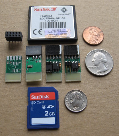
This is from the front page of my website, where you'll find more description. The SPI-10 connector spec for tiny SPI modules is very hobbyist-friendly. I see that DirtyPCBs dropped the .005" trace/space saying they were having too many problems with it. I wonder if that was associated with the ok but less-than-perfect product I described above. These last boards did not have the minor flaws that the first ones did. Maybe they quit using one of their suppliers that talked big but didn't do well. After these, I got another bunch of tiny prototype boards done by DirtyPCBs for work, and they were flawless.
I expect to do several more boards this year there. One planned is a 3U Eurocard, probably 4-layer.
http://WilsonMinesCo.com/ lots of 6502 resources
[Updated on: Wed, 04 January 2017 21:33] Report message to a moderator |
|
|
|
|
|
|
|
|
|
|
|
|
|
|
|
| Re: Getting boards fabricated [message #2130 is a reply to message #1624] |
Tue, 28 March 2017 14:41 |
mikemac
Messages: 249
Registered: March 2017
|
Senior Member |
|
|
Has anyone used any of the USA based PCB houses? Just curious if they're worth the extra cost. They do seem to be faster than China.
According to PCBshopper.com, I can get 5 of my 4.25x6" M68K boards for $43 and have them in a week! Better than I was expecting!
Mike
|
|
|
|
|
|
| Re: Getting boards fabricated [message #2143 is a reply to message #2135] |
Wed, 29 March 2017 18:39 |
plasmo
Messages: 876
Registered: March 2017
Location: New Mexico, USA
|
Senior Member |
|
|
I've had very positive experience with fabrication of 3 designs of pc board by Seeed Studio. The boards were all 2-layer, 100mm x 100mm and were $10 for 10 boards. Shipping were by DHL and was $20 for 10 boards or $24 for 20 boards. I had them fabricated in two separate runs. First run of 10 boards was sent off Monday and received Wednesday of following week. The 2nd run of 20 boards (2 designs) was sent off Sunday night and received next Monday afternoon. They are all superbly fabricated. The pc board layout tool I used was a 20-year old Winboard & Windraft. I followed Seeed Studio's format and naming convention and view them with their on-line Gerber viewer. It all worked amazingly well. The quality, cost, and speed of pcb fabrication is a revelation to me. It probably is old news to y'all, but this will fundamentally change how I design and prototype.
[Updated on: Wed, 29 March 2017 18:40] Report message to a moderator |
|
|
|
| Re: Getting boards fabricated [message #2167 is a reply to message #2143] |
Thu, 30 March 2017 15:53 |
mikemac
Messages: 249
Registered: March 2017
|
Senior Member |
|
|
Dumb question: when a PCB fab house says "Smallest Holes: 0.30mm" are they including the size of the vias in that restriction? 12mil vias seem awfully big.
Mike
|
|
|
|
| Re: Getting boards fabricated [message #2170 is a reply to message #1057] |
Thu, 30 March 2017 17:43 |
Garth
Messages: 29
Registered: April 2016
Location: Southern California
|
Junior Member |
|
|
Quote:Dumb question: when a PCB fab house says "Smallest Holes: 0.30mm" are they including the size of the vias in that restriction? 12mil vias seem awfully big.
That's finished hole size (ie, after thru-plating), and they don't care if it's a via or a component hole--although I don't know of any components that will fit in that small of a hole. After tolerance is taken into account, you couldn't even consistently get a wire-wrap wire into that size of hole. For .062"-thick board, that's an aspect ratio of about 5:1. I doubt that they would have trouble drilling a greater aspect ratio (especially since they usually stack boards and drill more than one at a time), but it gets harder to reliably thru-plate such a long tube. More-expensive board houses can do 8:1, or, if you want to pay, use a laser to make a .002" hole. (Yeah, it gets expensive; and I think the result is like a wire, not a tube, ie, it will be plugged.) If you go for a thinner board, a smaller hole should be no problem. I often do .032"-thick boards for work when I do very dense postage-stamp-sized SMT boards, and then I do .008" vias.
http://WilsonMinesCo.com/ lots of 6502 resources
|
|
|
|
|
|
|
|
|
|
| Re: Getting boards fabricated [message #2174 is a reply to message #2173] |
Thu, 30 March 2017 20:28 |
mikemac
Messages: 249
Registered: March 2017
|
Senior Member |
|
|
I'm OK with the sizes if the PCB fab house is!
But that brings up a good point: they don't specify what files they want. In particular, Gerber or Excellon for the drill file. Nor do they specify what layers they want Gerbers for. OK, I found the specs and the file list under their tutorial for their web based design tool. Yes, this is EasyEDA.com for those who haven't guessed yet. So we can ignore this paragraph.
KiCAD created two drill files for my board. One named M68K.drl which is expected. But it also created a second one named M68K-NPTH.drl that contains the four mounting hole size and locations. Should I merge the two or let EasyEDA do that?
As you can tell, I've never sent a design off to China to get made before. My limited experience is with US based PCB fab houses and they told me what they wanted up front. I was also using OrCAD so they could tell me exactly what to put where.
So thanks to everyone helping and putting up with me!!
Mike
|
|
|
|
|
|
| Re: Getting boards fabricated [message #2182 is a reply to message #2181] |
Fri, 31 March 2017 07:55 |
mikemac
Messages: 249
Registered: March 2017
|
Senior Member |
|
|
I used Eagle once to design a little LED board for the front panel of a computer I was building. It was small enough to fit within their limit for free use and I routed it by hand. It was very simple. My local board house held my hand on getting the files produced for fabrication. But that was the extent of my use of Eagle and that was almost a decade ago.
And it finally dawned on me that NPTH in the second drill file name stands for Non Plated Thru Holes! Duh! 
As soon as I generate the paste layer Gerbers, I think I'm going to risk the $43 on my 68K board.
Thanks again for the support!
Mike
|
|
|
|
 RetroBrew Computers Forum
 Members
 Search
 Help
Help Login
Login Home
Home


")
