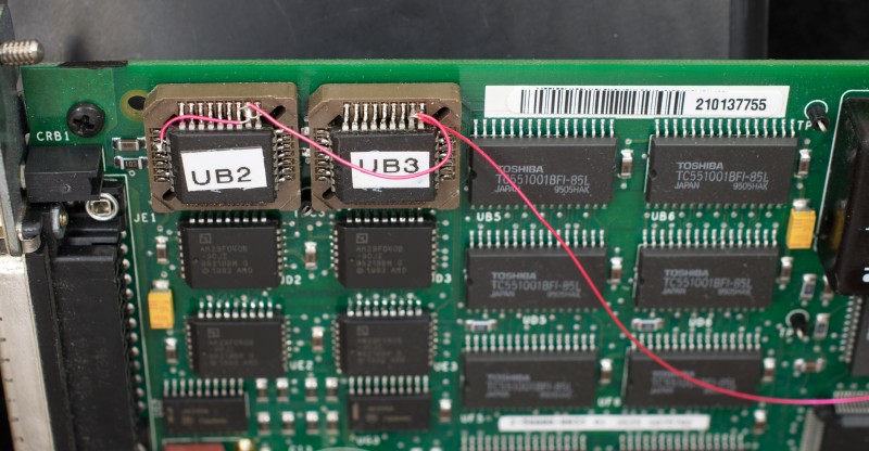
ADC SPX-MPU board
ADC Communication's SPX-MPU board is a MC68302-based controller board for the Soneplex communication product line. This board was phased out around 2005 and large number of them were available on eBay as surplus/salvaged boards. They are still available today (2017), although at a higher price of 15-25 USD.
SPX-MPU contains:
- MC68302 processor running at 16MHz,
- 3 banks of flash memory for a total of 2.25 megabytes,
- 4 banks of static RAM totaling 1 megabytes, the last bank of the RAM is backed up with a super capacitor,
- RTC72423 real time clock, backed by super capacitor,
- SCC68692 dual UART,
- 82C55 programmable peripheral interface,
- Discrete inputs and outputs.
Powering up the SPX-MPU:
There are at least two methods of powering up the board:
- Apply 30-48V to the DIN 41612 connector. One lead of the power goes to pin A1 & C1 while the other lead of the power goes to pin A32 & C32, the polarity of the leads are not critical. A on-board full-bridge rectifier will present the correct voltage polarity to the DC-DC regulator.
- Apply 5V directly to the circuitry. There are a number of test points on board that are hard wired to ground: TPC3, TPI1, TPF9, TPA13, and TPE7. Any of them may be used as the ground return. There are no readily available 5V hookup point, but two suitable locations are 1, the banded terminal of the 10uF tantalum capacitor directly behind the DB25 connector or 2, the '+' output of the DC-DC regulator. When 5V is applied directly to the board, the expected power consumption is between 180mA to 250mA.
When power is applied, the status LED on the front panel will turn orange for about 15 seconds and then it will turn green. With a null modem serial cable connected to the front panel DB25 connector, baud rate at 9600, 8N1, the following message will be displayed “ Welcome to ADC: Soneplex Shelf Interface ”, etc
———photo of screen shot—
Repurpose the board
Note: once the board is modified it will no longer referred as the SPX-MPU since it is no longer operated as the manufacturer intended. It will be referred as MPU302 or “the board”.
Perhaps there is a way to upload software patch into the board, but I have no knowledge of it. In the absence of software upload, the most obvious way of changing software is to replace the boot flash with a new set of boot flash. The boot flash are located on the corner of the board above the DB25 connector. UB2 is the most significant byte and UB3 is the least significant byte. For people with the appropriate skill and equipment, UB2 and UB3 can be readily cut out and sockets installed in their place. New boot software can be programmed in an external flash programmer and installed in the sockets. The board will now boot up with the new software. The drawback with this method is that every board repurposed need to remove two flash chips, install two sockets and program two new flash chips. That's a significant effort in time and money. There is another way:
 Photo of bootflash replaced with sockets
Programming headers for 68302SBC
The programming headers are a pair of flash chips (different manufacturer than the ones soldered on board) with the appropriate boot software programmed and then soldered to the solder tabs of PLCC sockets. This sub-assembly will fit over UB2 and UB3. A single-pole double-throw switch is wired to boot chip select and can select either the original boot flash or the programming headers.
 Photo of programming headers installed
Photo of programming headers removed
Detailed view of the programming header installed over the existing boot flash
Yet another way of replacing the original boot software is to program a set of flash with the desired boot software, straighten the 'J' leads of the custom flash chips and position them on top of the original flash chips, solder the corresponding leads except the chip selects. A single-throw double-pole switch selects either the chip selects of the original flash chips or the chip selects of the custom flash chips. This arrangement is for boot flash software development; if boot flash software crashed and won't boot at all, the developer can switch to the custom boot flash and regain the control of the board.
Photo of custom boot flash 'piggyback' over original boot flash
Detailed view of the 'piggyback' of the custom boot flash chips
The software for the programming headers works as follow: switch the boot chip select to the programming headers and power up. MC68302 will execute the new boot software located on the programming headers. Load a cloning software into the 68302SBC RAM and execute it. This cloning software will copy the boot software located on the programming header into RAM and then examine the device ID of the flash continuously and wait for the switch to connect to the original boot flash. Once the switch to the original boot flash is made, the cloning software will erase the flash and copy the new boot software into the original boot flash. The repurpose of the board is now completed.
This method still requires some soldering/desoldering:
- The smt capacitor between UB2 and UB3 needs to be removed, otherwise the headers will not fit properly
- The 330 ohm resistor connecting boot chip select need to be removed and a pull up resistor installed at the flash side of the chip select
New boot source code, S-record
cloning software source code, S-record
ADC SPX-MPU schematics
ADC SPX-MPU connector definitions
Photo gallery
Software collection


